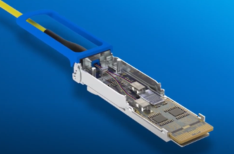
Transceivers Requirements and Technology Development Direction

Transceivers needs are driven by telecommunications, but even more so by large-scale data centers, where the demand for transceivers is increasing alongside high-speed demand.
Nowadays, transceiver requirements can be broken down into 6 key characteristics: Low cost, high speed, high density, low power consumption, short lifespan, and narrow temperature range.
- Low cost: With large-scale deployment comes a high quantity of transceivers. Therefore, it’s crucial that transceivers are as cost-effective as possible to manage their deployment within data centers.
- High speed: Data centers must meet the demand for 4K VR, Internet of Things (IoT), and cloud computing, significantly increasing bandwidth requirements.
- High density: The goal is to increase the number of optical transmission channels in a unit space and improve data transmission capacity.
- Low power consumption: Sustainability practices are now widely adopted to protect the environment. Lower power consumption also reduces operational expenses compared to older high-power modules.
- Short lifespan: Rapid development and increased data communication mean optical modules typically do not need to operate for more than 3 to 5 years.
- Narrow temperature range: Data centers operate in controlled environments (temperature and humidity), necessitating optical transceivers designed to function between 15°C and 55°C to meet current requirements.
These 6 characteristics enable transceiver manufacturers to introduce new technologies and methods tailored to meet evolving standards and application conditions. Let’s review some new techniques based on these requirements that can facilitate the development of large-scale data centers.
A. Non-hermetic packaging
60% of the total cost of a transceiver comes from optical components, and cost reductions on optical chips are increasingly challenging. Therefore, transitioning from hermetic to non-hermetic packaging significantly reduces costs while ensuring transceiver performance and reliability.
Non-hermetic packaging involves making the optical device itself not airtight, optimizing optical component design, using different packaging materials, and improving the packaging process.
Of course, the laser component poses the greatest challenge, but manufacturers have developed lasers capable of operating in non-hermetic applications to address this issue.
B. Integrated technology (hybrid)
Current transceivers must transmit more data than ever before. Photonics integration meets this demand by integrating silicon-based or indium phosphide-based components. Hybrid technology refers to integration using different materials.
Hybrid integration combines free-space optics and integrated optics. This approach can be highly compact, and automated processes can easily support mass production.
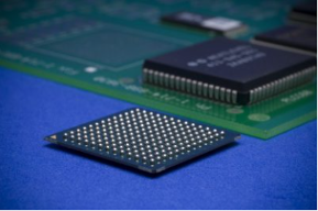
C. Flip Chip technology
Flip chip technology is a high-density chip interconnection technology from the integrated circuit packaging industry. It addresses the trend toward smaller chip sizes by directly soldering the optical chip onto the substrate using gold-gold or eutectic soldering, which is superior to wire bonding (short distance, low resistance, etc.).
Flip chip technology is valued for its high precision, efficiency, and quality, making it widely used in the optical module industry
Flip Chip technology is valued for its high precision, efficiency, and quality. That’s why it is widely used in the optical module industry within data centers.
D. Chip-on-Board (COB) Technology
COB technology is also used in the integrated circuit packaging industry. Its principle, like that of non-hermetic packaging, involves directly attaching chips or optical components to the PCB, followed by electrical connections bonded with gold wires, and finally applying adhesive on top.
The major advantage of this technology is that all steps can be automated, which is why it is widely adopted, primarily for short-range applications (SR4, AOC, etc.), but it is gradually moving into long-range applications (LR4).
E. Silicon Photonics Technology
Silicon photonics is a technology involving optoelectronic device technology and silicon-based integrated circuits integrated on the same silicon substrate. Silicon photonics technology can be used in many cases, but from an industry standpoint, performance and cost competitiveness drive new technologies, which is where the challenge lies.
Today, the demand from data centers for low-cost, high-density products presents numerous opportunities for silicon photonics-based applications.
What about standards?
Whether it’s MSA or IEEE, none of them defines how to build an optical transceiver, which means for the same standardized transceiver, multiple solutions can exist, each with different prices.
This is where caution is necessary because the application for which we need to use a transceiver depends on the performance that the transceiver must achieve. In other words, we cannot use the same transceiver for all applications. For instance, using a non-hermetic package for a telecom application may not be suitable considering it might not be placed in a controlled environment.
This is the daily challenge for a third-party transceiver manufacturer like Skylane Optics: convincing people that price isn’t everything and helping our customers choose the right solution (transceivers) for their application. Indeed, three of the characteristics we discussed in this article (low cost, short lifespan, and narrow temperature range) are geared towards the world of data centers but pose significant challenges for the telecommunications sector, and this needs to be considered.
In conclusion, the direction of transceiver technology development is largely influenced by large-scale data centers, and the industry responds by offering multiple technologies to meet the current and future needs of these data centers. This results in multiple solutions and varying costs for the same standards.
—-
Source: Echo Brown: The Technology Development Direction of Data Center Optical Transceivers
Want to know more about our company? our products?
Boost your networks with intelligent SFP+ transceivers, from 1G to 10G!

Powering AI and ML with Skylane Optics’ High Speed DACs

The importance of effective data center cabling management!
